


product
The products are mainly used in the Ⅱ-Ⅲ generation semiconductor, 5G communication, OLED display, AR, VR, aerospace and other fields.
- PBN Division
- PG Division
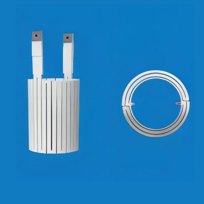
- Composite Heater Division
- Refractory Metal Products Division
- Other Ceramics
-
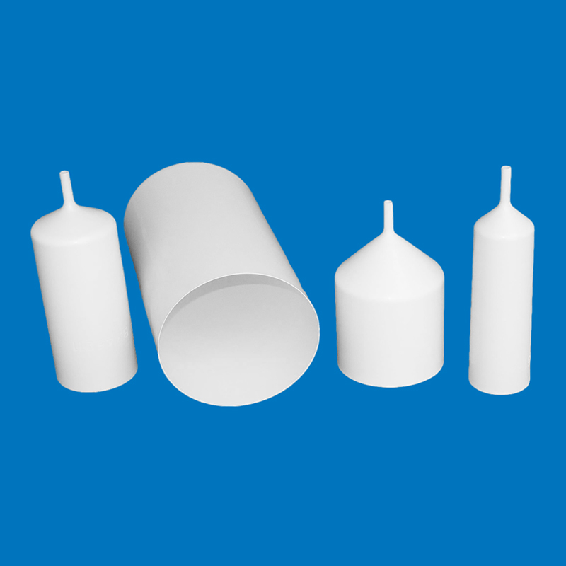
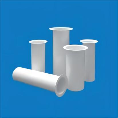
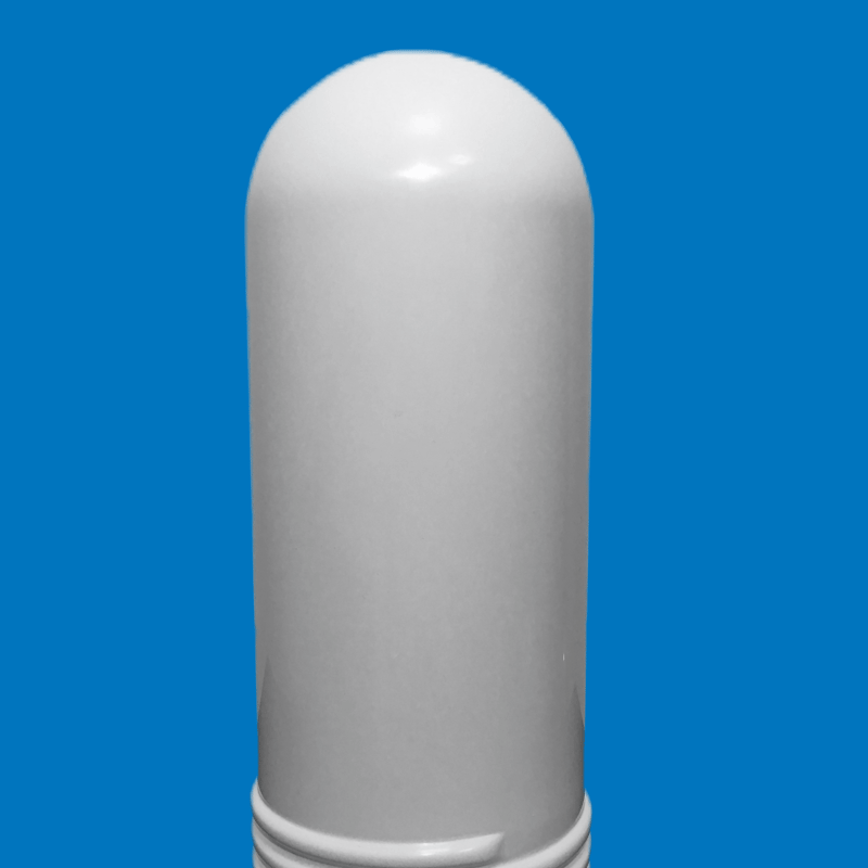
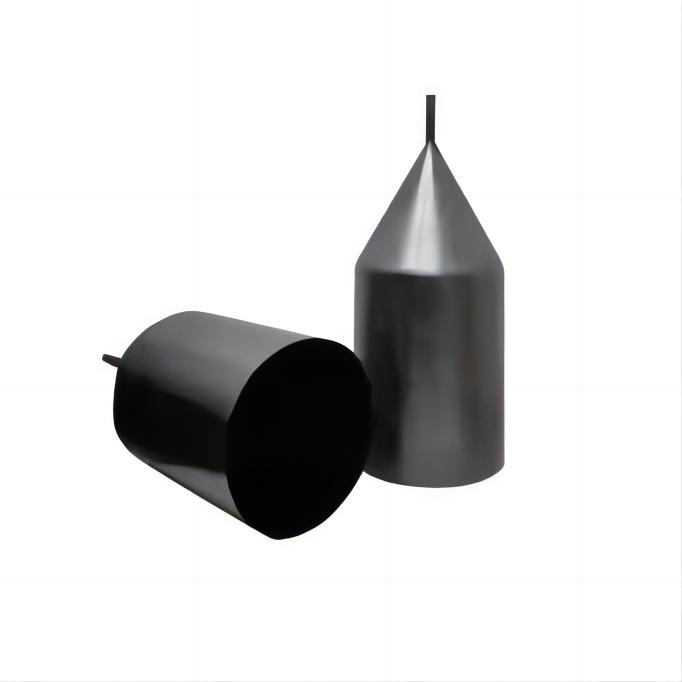
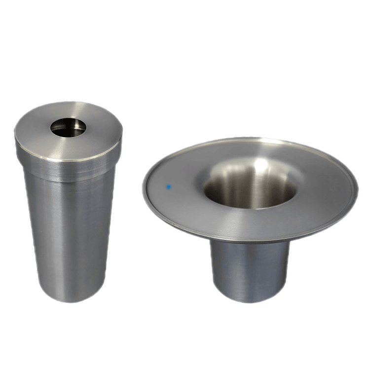
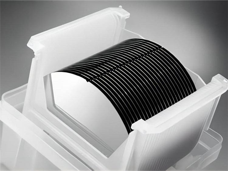
VGF PBN Crucible, Pyrolytic Boron Nitride Crucible
-
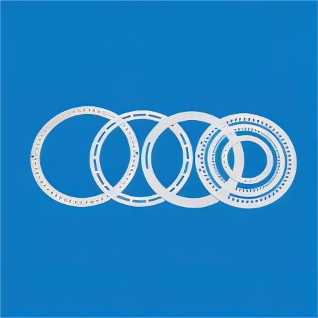
PBN Ring Pyrolytic Boron Nitride (PBN)
-
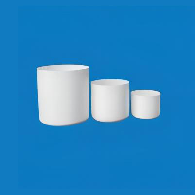
OLED Crucible Pyrolytic Boron Nitride (PBN)
-
PBN Coating Pyrolytic Boron Nitride (PBN)
-
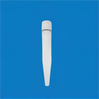
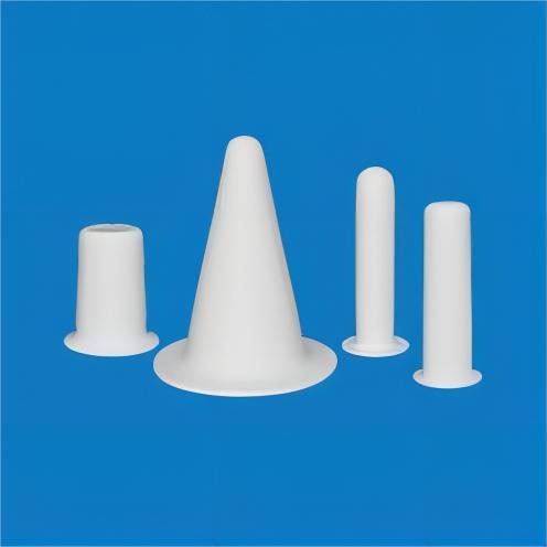
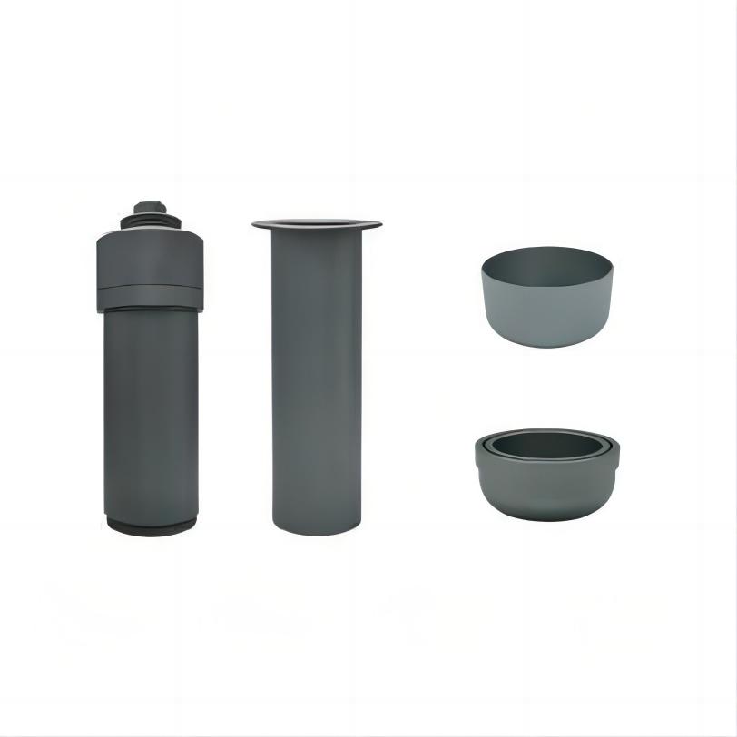
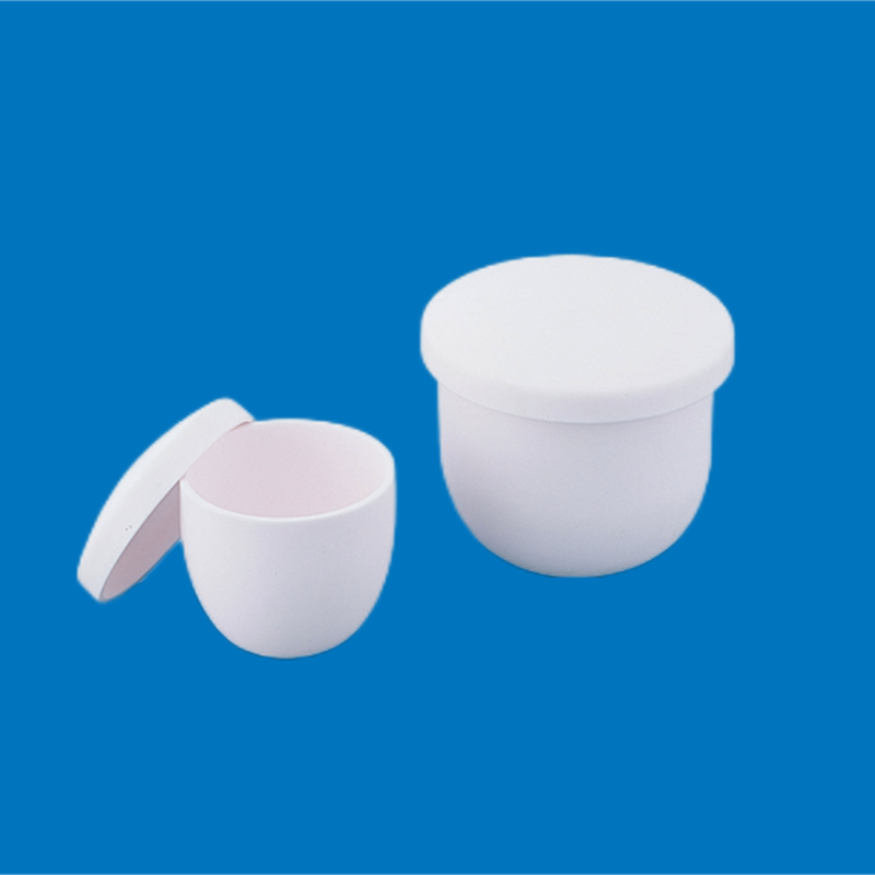
PBN Machined Parts Pyrolytic Boron Nitride (PBN)
-
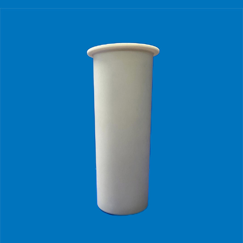
LEC Crucible Pyrolytic Boron Nitride (PBN)
-
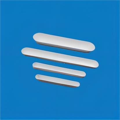
PBN Boat Pyrolytic Boron Nitride (PBN)
-
MBE Crucible Pyrolytic Boron Nitride (PBN)
-
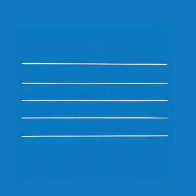
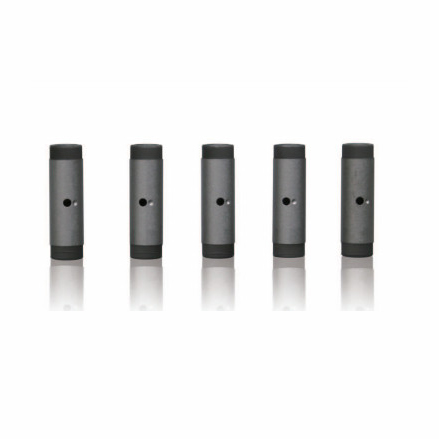
PBN Rod Pyrolytic Boron Nitride (PBN)
-
CIGS Crucible

our projects
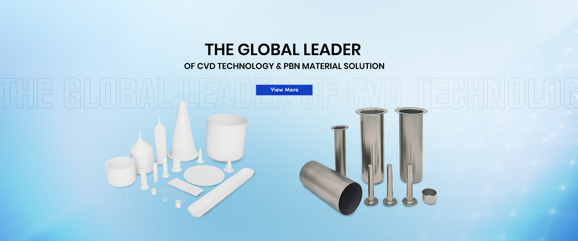
It is an outstanding solution expert of PBN and CVD technology.
-

Who We Are
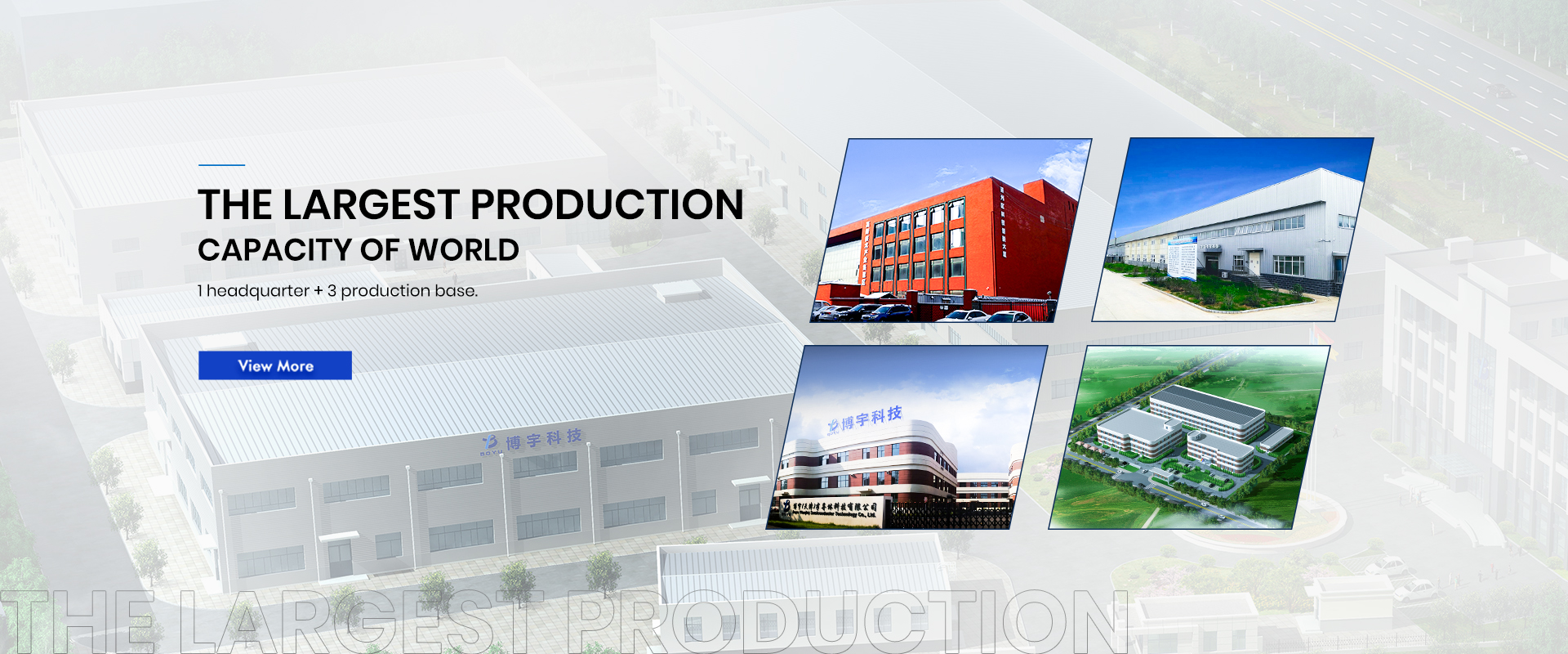
Beijing Boyu Semiconductor Vessel Craftwork Technology Co., Ltd. was established in 2002, located in Beijing Tongzhou Economic Development Zone, which is the first large-scale PBN manufacturing enterprise in China.
-

Our Business
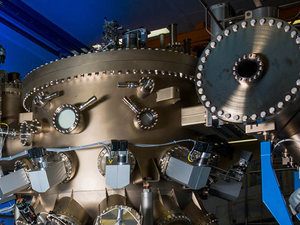
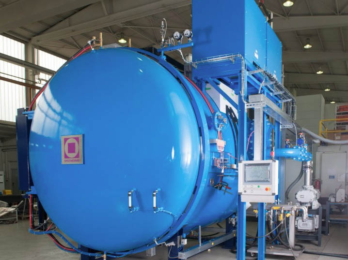
We focus on the design, development, production and sales of CVD products such as ultra-high purity, high thermal conductivity, thermal shock resistance, dense pyrolytic boron nitride (PBN) and pyrolytic graphite (PG).
-

Our Mission
"Create value for customers, win-win cooperation!" is the professional belief of every Boyu person. Focus on every product and win the trust of every customer!
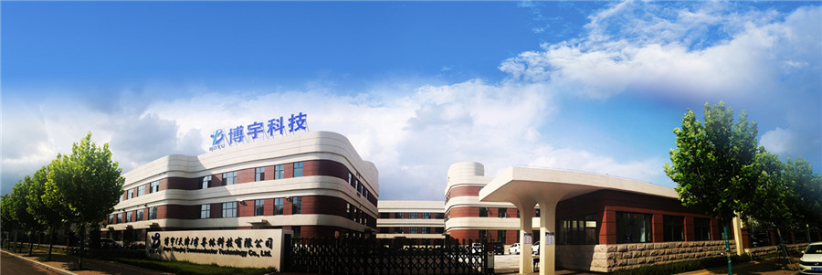
Beijing Boyu Semiconductor Vessel Craftwork Technology Co., Ltd. was established in 2002, located in Beijing Tongzhou Economic Development Zone, which is the first large-scale PBN manufacturing enterprise in China, with more than 310 employees.